Articles
Plasma Application to Solar Cell and PCB/FPCB Industry l PSM
by Professional Writer Professional Writer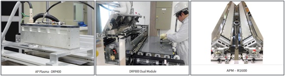
PSM Co., Ltd. has led the development of atmospheric pressure plasma technology
through constant technological
innovation for more than 20 years since its foundation in 2001. PSM is now
leading the global market with the core atmospheric plasma technology based on
such accumulated expertise.
Through its technological prowess, PSM has grown into a world-class plasma company that is well recognized in the global market as well as the Korean domestic market in various industries.
PSM plasma technology and equipment application to Solar Cell/Industrial Sunglasses
PSM plasma technology reduces the concentration of chemicals by applying a DRP electrode to the thin-film solar cell chemical cleaning process in an environment-friendly way, and itis also applicable to pre-treatment of smart glass coating for architecture glass.
Great advantages of PSM’s DRP electrode
ü It can reduce chemical concentration in the environment-friendly alkaline cleaning process
ü It can improve
the production yield by increasing the reliability of thin-film coating
ü It can clean the contaminated glass substrate for Solar Cell Panel and Smart Glass
ü It can remove suction marks, pin marks,
watermarks on displays and architectural glass
panels, and so on
ü It can remove residues of Nano-coating
film used to protect the surface such as AF
ü It has very high cleaning effect five times higher than AP electrode
ü It has wide electrode and sample spacing of up to 12 mm Max.
ü I can be connected in series to be applied to large sample panels
PSM’s various Plasma Application processing in PCB/FPCB Industry
PSM’s AP Plasma M electrode (APM) can be effectively applied to the pre-treatment process for PCB
substrate plating and the surface treatment process before SMT/Flip-chip
bonding and also applied to the surface treatment process for flexible PI film substrate and polymer substrate.
It is possible to be used in low-temperature processing below 40℃, and it does not require consumable parts.
And AP plasma roll-to-roll equipment can be applied to the surface treatment process for
FPCB FCCL PI films and vacuum plasma equipment is also can be used in the PCB decontamination process.
Along with such applications, PSM provides vacuum plasma de-smear processing in PCB/FPCB Industry. In addition to de-smearing processing, various plasma treatment processes are possible, which enables the hydrophilic surface modification and reduction process, and so on.
Great advantages of PSM’s APM electrode
ü It performs the uniform removal of smear of epoxy residues generated during the PCB
drilling process and secures
product reliability
ü It consumes a small amount of gas and has a low running cost due to no chemical disposal expenses. vacuum plasma technique
Click here to contact us.
View more: PSM Plasma Application AreaSponsor Ads
Created on Jul 8th 2021 00:10. Viewed 156 times.