Origin PCB-An Innovative Enormous Breakthrough
Abstract
The origin of Printed Circuit Boards (PCB) is traced back to the 20th century and they were first used in in the 1900s. The very first Boards were made of materials such as Masonite, thin planks of wood before Printed circuit boards came into use.PCBs are used in providing mechanical support and the electronic connection between components of an electronic device. Pads and conductive tracks among other elements are used in these connections. Origin PCB can be made of a single layer of copper (single sided), two layers (double-sided) or even have multiple copper layers. Connections between the copper layers are made using plated through holes (vias).
Content
Origin PCB
Printed Circuit boards were invented by Paul Eisler, a Vienesse inventor, an engineer in 1936. In terms of Origin, PCB was, made in England as components of a radio set. Before the invention of PCBs, point to point constructions were used in the electronic device.
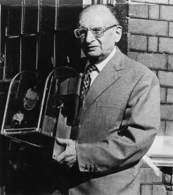
Paul Eisler
The point to point connections was not efficient, their designs were bulky and could not be relied on. In 1943 the Printed circuit board technology was adopted in the USA and was used on large scale in the production of proximity fuses which were used in the Second World War. PCBs proved to be more efficient and reliable compared to point to point connections that were used earlier on. From the time PCBs were invented, they became more useful in the mid-1950's following the development of auto assembly process by the Army of the United States.
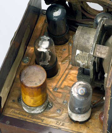
Rado with First PCB
Origin PCB elements had wire leads and holes were drilled on the boards through which the wire leads passed. The wire leads would then be soldered on the PCB trace. This was referred to as the through-hole method of PCB assembly. Further innovations and inventions were made and in 1949, the Auto Assembly procedure was developed by Stanislaus F. Danko and Moe Abramson. Both Stanislaus and Abramson belonged to the United States Army Signal Corps. In 1956, they received the patent for their development but this belonged to the Army of the United States. The fabrication of printed circuit boards which is in use today was developed. It evolved from etching and lamination techniques that were developed earlier on.
PCB fabrication process involves soldering which is done by passing a PCB through a wave or ripple of solder in molten form. The procedure is automatic and a wave soldering machine is used. The drawback of this method is some materials are wasted; the wires protruding from the surface are merely cut. Drilling of holes is also costly.
Conclusion
Further innovations in the PCB electronic devices will lead to the production of miniature products with greater reliability and efficiency. Future developments may include greater use of Package on Package (POP), molded plastic boards with three dimensions and integrated circuit chips. These developments coupled with other innovations will create a more dynamic and evolved PCB electronics industry.
You can also see this video to get full idea about the Origin of PCB
https://www.youtube.com/watch?v=mb6KnEae5Mw
Post Your Ad Here
Comments