Articles
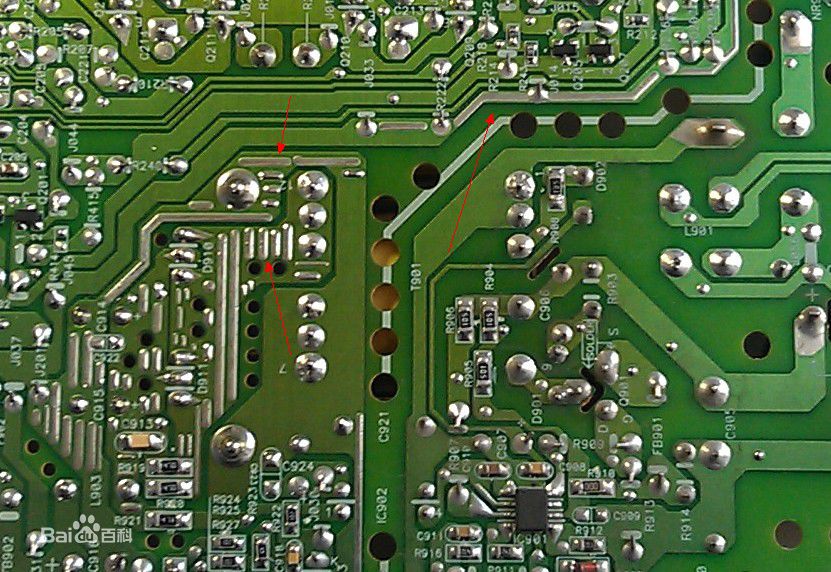
Solder mask
by Warren C. Electronics EngineerThe solder layer refers to the printed circuit board to the green part. In fact, the solder layer is negative output, so the shape of mapping in the solder layer to the board, and not on the green solder, but with copper. It usually in the reflow soldering process control during welding defects in the role is important, PCB designers should try to reduce peripheral pad spacing or air gap characteristics.
Solder mask comes in different media depending upon the demands of the application. The lowest-cost solder mask is epoxy liquid that is silkscreened through the pattern onto the PCB. Other types are the liquid photoimageable solder mask (LPSM or LPI) inks and dry film photoimageable solder mask (DFSM). LPSM can be silkscreened or sprayed on the PCB, exposed to the pattern and developed to provide openings in the pattern for parts to be soldered to the copper pads. DFSM is vacuum laminated on the PCB then exposed and developed. All three processes typically go through a thermal cure of some type after the pattern is defined although LPI solder masks are also available in Ultra Violet (UV) cure.
Sponsor Ads
Created on Feb 28th 2018 04:32. Viewed 423 times.