Articles
Printed Wiring Board-An Attractive Fundamental Introducing
by Warren C. Electronics EngineerAbstract
The printed wiring board (PWB) also known as Printed Circuit Board (PCB) is the essential part of every electronic device. The printed wiring board was introduced in early 1950’s,which was the building block for the electronic packaging.The important feature of the printed wiring boards is to get maximum components count per square inch of PWB. This is known as component density. Hence many advanced packaging techniques were introduced like Ball Grid Array (BGA), Chip Scale Packaging (CSP) and Chip on Board (CoB).
Content
1.The main factors affecting the performance of PWBs
1.1 Speed of operation of the printed wiring board
1.2 Power Consumption
1.3 Thermal Management
The surface mount components are miniature size and are extensively used in many PWBs to provide maximum component density while maintaining electrical, thermal and signal integrity performance of the device.There is variety of materials used for PCB substrate, the most common is FR4.The below shown figure-1 shows the evolution of Computer CPU and associated PWBs.
1.The main factors affecting the performance of PWBs
1.1 Speed of operation of the printed wiring board
The speed at which the electronic device operates is a very important factor in the design of PWB interconnections. The speed of the signal propogation is inversely proportional to the square root of dielectric constant of substrate material of PWB. Time of flight is the propagation time of the signal which is directly proportional to the length of conductors and must be kept short to ensure optimum electrical performance of a system. Above 25MHz the PWBs use the strip-lines and micro-strips for this purpose.
1.2 Power Consumption
Increasing clock rates, increasing number of gates will result in increasing power consumption. The special care must be taken for high speed switching circuits where ground return current flow is to be channeled in optimum fashion. The separate ground plane must be made in multilayer PWBs to ensure low resistance current flow. A separate bus bar system is also preferable for high power circuits.
1.3 Thermal Management
The PWBs are poor conductors of heat so a proper care must be taken to use methods to dissipate the heat generated by power components in PWBs. Heat sinks, heat vias, conductive planes in PWBs and metal slugs are good techniques.
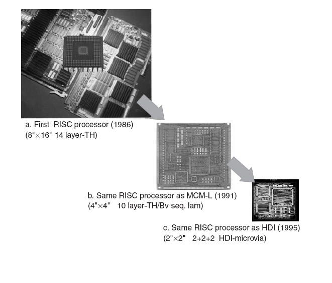
FIGURE - 1
Sponsor Ads
Created on Mar 20th 2018 05:36. Viewed 266 times.