Articles
How To Make A Multilayer PCB
by Howie Liu Electronics EngineerAbstract
Most quick PCB Prototypes are usually 2 layer PCBs. This is because they are cheap to manufacture and they can even be made at home. In addition, it is also very easy to design and most PCB Design software allow you to design a 2 layer PCB for free! As the PCB Components becomes smaller and smaller each time, the demand for small sized PCB goes higher and higher. Designing a 2 layer PCB with these kind of components becomes complicated and sometimes impossible, especially if you have a few BGA PCB components to route! This is where the multilayer PCB comes in handy. However, switching from a 2 layer PCB designer to a multilayer PCB designer is not always a piece of cake. There are a few things you must know.
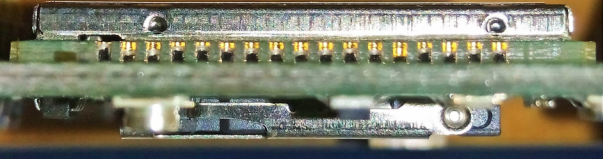
When making multilayer PCB, it is important to understand Vias and how they work. There are three major types of Vias; Blind vias, Buried vias, and Through vias. Through vias that are connected to the internal layers are called Stub vias. Just like the name suggests, Buried vias are submerged within PCB layers, and never appears on the outside layers. Buried vias connect a signal between layers that a through via cannot reach. On the other hand, blind vias connect a signal from the outside layer to any internal layer but does not go all through the board. To keep the multilayer PCB cost effective, blind and buried vias should be used only when they are really needed. Knowing how to use all these types of vias in a multilayer PCB is a very important step for multilayer PCB design, since it makes PCB routing to be incredibly easier. With vias in a multilayer PCB, PCB Components can occupy a much smaller space. Still, signal integrity for the multilayer PCB will be much more improved since the trace distance will be significantly reduced. Blind vias are usually laser-drilled microvias of about 0.1mm. This means that these microvias can be placed on multilayer PCB pads. However, vias on a BGA pad should be avoided as much as possible.
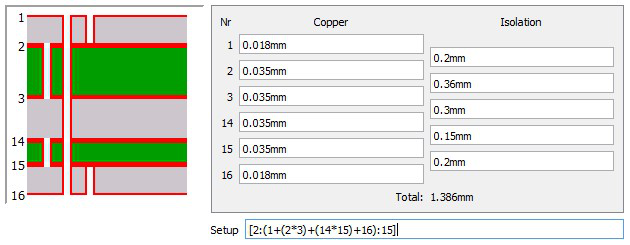
When designing a multilayer PCB, it is advisable to start by ensuring that the design rules are well set. This involves planning and knowing which layers shall have what type of via. For example, in Eagle CAD software, the following representation is used: p ∗ q means that layer p and q are combined with a core, while p + q means that these two layers are combined with prepreg. () signifies buried and through vias, while [a : ... : b] signifies blind vias. [2 : (1 + (2 ∗ 3) + (14 ∗ 15) + 16) : 15]
The above representation signifies a multilayer PCB setup that has two core and three prepreg combinations. As you can see, there is a buried via going through 2,3,14,15. Another important preparation is the PCB Stack-up plan for the multilayer PCB. This plan gives details about the main function of every layer in a given multilayer PCB. For example, for a four-layer PCB, you could stack up the layers as follows:
Layer 1: Signal traces
Layer 2: +3.3V DC
Layer 3: GND
Layer 4: Signal traces
Sponsor Ads
Created on May 3rd 2018 22:46. Viewed 313 times.