An introduction to PCBs
Printed circuit boards (PCBs) appear in almost every electronic device. If there are electronic parts in a certain device, they are also mounted on different sizes of PCB. In addition to fixing various small parts, the main function of the PCB is to provide mutual electrical connection between the parts above. As electronic devices become more complex and require more and more parts, the lines and parts on the PCB are becoming more and more dense. The bare board (with no parts on the top) is also often referred to as the "Printed Wiring Board (PWB)."
The substrate of the board itself is made of a material that is insulated and heat-insulating and is not easily bent. The thin circuit material that can be seen on the surface is copper foil. The original copper foil is covered on the whole board, and part of the manufacturing process is etched away, and the remaining part becomes a mesh-like small line. These lines are called conductor patterns or wires and are used to provide electrical connections to the parts on the PCB.
To secure the parts to the PCB, we soldered their pins directly to the wiring. On the most basic PCB (single panel), the parts are concentrated on one side and the wires are concentrated on the other side. In this case, we need to make holes in the board so that the pins can pass through the board to the other side, so the parts are soldered to the other side. Because of this, the front and back sides of the PCB are called the Component Side and the Solder Side.
If there are some parts on the PCB that need to be removed or replaced after the production is completed, the part will be installed with a socket. Since the socket is directly soldered to the board, the parts can be detached at will. Seen below is the ZIF (Zero Insertion Force) socket, which allows the part (here referred to as the CPU) to be easily inserted into the socket or removed. A fixing rod next to the socket that secures the part after you insert it.
If you want to connect two PCBs to each other, we usually use the edge connector called "Golden Finger". The golden finger contains a lot of bare copper pads, which are in fact part of the PCB layout. Usually when connecting, we insert the gold finger on one of the PCBs into a suitable slot on another PCB (generally called the expansion slot Slot). In a computer, such as a display card, a sound card or other similar interface card, it is connected to the motherboard by a gold finger.
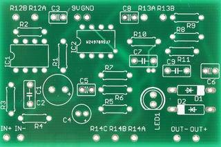
The green or brown color on the PCB is the color of the solder mask. This layer is an insulating protective layer that protects the copper wire and prevents the part from being soldered to an incorrect location. A layer of silk screen is additionally printed on the solder mask. Text and symbols (mostly white) are usually printed on this to indicate the position of each part on the board. The screen printing surface is also referred to as the legend.
If you want to learn more about IC, visit: IC Chip Word
Post Your Ad Here
Comments