8 Major Steps To Semiconductor Wafer Fabrication
However, an integrated circuit (IC), also called a semiconductor chip, can imitate you with the fingernail-sized type aspect, it is always full of millions of electrical components—transistors, diodes, resistors, and also capacitors—which almost all work together to do logic procedures and save data files.
Thus, just what will it choose to use manufacturing this type of circuit, when you ask?
The technology behind mechanism an IC is going significantly beyond the basic setting up of different elements. Actually, microscopic circuit patterns are created on several layers of numerous components, and also just after these actions are continued a few hundred times is the chip after all finish.
Nowadays, we are now presenting a unique series which will walk you over the producing method of this innovative machine, from the raw material phase to the finalized tests of the semiconductor chip. The series will possibly include 8 elements and will be released per week.
Read on for the first part of the series, which introduces the “canvas” for integrated circuits, otherwise known as the silicon wafer.
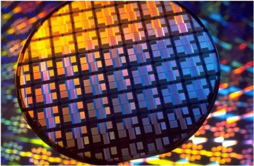
What’s a wafer?
A wafer, also known as a disc, is a slim, shiny piece of a silicon rod which is slice with precise diameters. Almost all silicon wafers are made from silicon recovered from sand. The major advantage of utilizing silicon is usually that this is rich in source, becoming the richest element naturally, right after oxygen. the eco-friendly characteristics are a further benefit.
Making an ingot, the base for wafers
When silicon is taken out from sand, it requires to be refined before it might be used. Initially, it gets heated up until it melts into a high-purity liquefied and then solidified into a silicon rod, or even ingot, utilizing typical developing techniques such as the Kochanski (chokh-RAL-skee) technique and also the Floating Zone technique.
The preferred Czochralski technique utilizes one small part of solid silicon (seed) that is used in a shower of molten silicon, or even polycrystalline silicon, then slowly but surely dragged in turning when the liquid gets a cylindrical ingot. For this reason, the completed wafers are generally round discs.
Presenting unique definition to the phrase “wafer-thin”
Before it's fully cooled, the cone-shaped finishes of the ingot are cut-off when the entire body is divided into small wafers of equal thick-ness with sharpened diamonds saw cutters. This describes exactly why an ingot’s diameter will eventually figure out the dimensions of a wafer. In earlier days of the semiconductor company, wafers were just three inch in size. After that, wafers are increasing in proportions, as larger wafers lead to much more chips and also better efficiency. The largest wafer size used in semiconductor manufacturing nowadays is twelve inch, or even 300mm.
Smoothing things out – the lapping and also sharpening procedure
Divided wafers have to be prepped before they are production-ready. Rough chemical compounds as well as equipment polish the unequal surface of the wafer for a mirror-smooth finishing. The perfect surface enables the circuit patterns to printing much better on the wafer area throughout the lithography procedure, which we'll cover in a later posting.
Post Your Ad Here
Comments