Articles
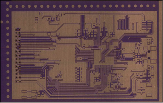
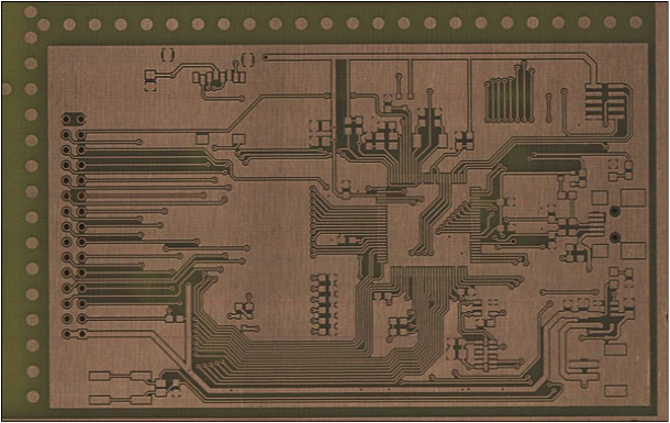
PCB Thickness
by Howie Liu Electronics Engineer
The technology of PCB is not one that is at a standstill rather it has been evolving from level to level and from one stage to another different upgraded stage. As the PCB technology changes, it has been discovered that connecting all the needed components into standoffs to a PCB is very strenuous. This motivated researchers to find a less labor intense procedure and this brought about the single-sided circuit boards.
The first PCBs were designed simple and with the single sided board which were attached to various layers. The boards are made from thin insulating materials which are solid and a good insulator. As the PCB technology evolves continually, there came the dawn of multiple board connections. This type of connection needs two connectors for each one of the PCB. One will be for the PCB itself and the other for the rack. As the case may be, the standard PCB thickness of the material that is to be used is 63mils; it means that the corresponding rack connector should also match up to this thickness.
That is how the industry came to the standard PCB thickness that is specified to be 63mil.
Most times, the majority of the PCBs were not designed with edge connectors. For instance; single PCBs which are made for game products and the PC motherboards. There seems to be no reason to use the specified standard PCB thickness of 63mil to make these products as the 63mil specification was necessary to match up to the thickness of an edge connector. Since the layer counts for the PCBs were increased to match up to the wiring requirements of the more complex circuits, the circuit boards were also produced to have a higher layer counts. This brought about the jump from the standard PCB thickness of 63mils to 93mils.
However, with high-temperature materials, Isola's 370HR can be used in scores of 8, 10, 14, 22 or 39mils respectively. In other words, the standard PCB thickness depends on the layers of your foil lamination. If the foil lamination is for a four-layer PCB, the standard to be used should be .031+/-10%
For a six-layer foil lamination, the best standard to be used should be .062+/-10% or .031+/-10% respectively.
For 8 and ten layer boards, the standard PCB thickness is specified at 0.062, 0.093 and 0.125 inches.
Sponsor Ads
Created on Nov 28th 2017 03:54. Viewed 170 times.